
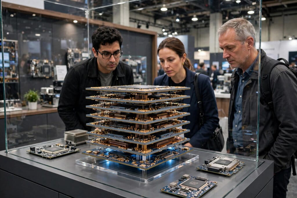
Samsung Electronics will use TSMC’s 3-nanometre process to produce the base dies for Nvidia’s next-generation custom high-bandwidth memory chips, Reuters reported on October 18, citing a report in the Seoul Economic Daily. The arrangement would mark the first time Samsung has worked with its Taiwanese foundry rival at the HBM manufacturing stage, according to the reports.

Neither Samsung, TSMC nor Nvidia has publicly confirmed the arrangement. The reporting, based on industry sources cited by the Seoul Economic Daily, says Nvidia asked all three of its main memory partners, Samsung, SK Hynix and Micron Technology, to use TSMC’s process for the NVHBM base dies, alongside sixth-generation DRAM technology for the core dies. The chips are the memory half of the hardware stack explained in our guide to NVIDIA’s AI chips.
What NVHBM Is: Nvidia’s Custom Memory Design
NVHBM is Nvidia’s proprietary custom version of high-bandwidth memory, unveiled in August. Its defining change is to integrate Nvidia’s custom memory controller directly into the base die, the logic layer that sits at the bottom of the HBM stack and determines data transfer speed, instead of leaving that controller on the GPU.
Moving those functions off the GPU frees space on the processor for additional computing circuits. To make room for the controller on the base die, the physical layer, the circuitry that exchanges electrical signals with external chips, was shrunk by 60% from standard HBM, the Seoul Economic Daily reports. The result, by the paper’s account, is memory bandwidth up to 30% wider and power consumption about 15% lower than standard HBM4E, the seventh generation of the technology.
That design is why an advanced logic process is needed at all. Packing functions relocated from the GPU into a small base die requires a 3-nanometre process with high yields, and the paper estimates TSMC’s 3-nanometre yield at more than 90%, against roughly 60% for Samsung Foundry’s comparable 2-nanometre SF2 process.
Why Samsung Accepted A Rival’s Foundry
Samsung has historically run an in-house turnkey model for HBM, making both core and base dies itself. According to the reports, it accepted Nvidia’s requirements after an internal review in order to secure its place in the NVHBM supply chain, while keeping its independent model for standard HBM products and for other customers.
Capacity is the second pressure. The Seoul Economic Daily reports that Samsung’s base die lines are limited to Hwaseong Line 17 and part of Pyeongtaek P3, a setup built for existing HBM demand that cannot easily absorb custom NVHBM volumes. TSMC, by contrast, told investors at its third-quarter briefing that it will add two new 3-nanometre lines at Fab 18 in Tainan, with further lines planned in Arizona and Kumamoto.
Samsung is also hedging. The reports say it is assessing whether its own foundry could produce NVHBM base dies if demand exceeds TSMC’s available capacity, and the Seoul paper reports Samsung Foundry is validating base die production on its own 2-nanometre process. The memory bottleneck behind the deal is the same supply story running through our explainer on why NVIDIA powers the AI boom.
The Shortage Behind The Deal: HBM Demand Up 91%
The context is a memory market that cannot keep pace with AI accelerators. Investment bank UBS, cited by the Seoul Economic Daily, projects HBM demand next year at about 61.5 billion gigabits, a 91% increase on this year, while new shipments from memory makers are expected to reach only about 54.6 billion gigabits, leaving a shortfall of roughly 10% against demand.
In that market, standardising the base die across Samsung, SK Hynix and Micron on one proven process lowers Nvidia’s verification burden and raises total supply, even if it means directing work to TSMC that Samsung would once have kept in-house. For context on how that supply chain feeds Nvidia’s results, see our explainer on how NVIDIA makes money from AI.
Why It Matters
The central entity is NVHBM, Nvidia’s custom memory, and the story matters because it shows where power now sits in the AI supply chain. Nvidia’s design requirements are strong enough to make Samsung, a vertically integrated giant that competes with TSMC in foundry, manufacture a core component on its rival’s lines, a first at the HBM stage. For Samsung, the choice protects its memory position at the cost of its foundry pride and margin. For TSMC, it extends its process lead from logic chips into the memory stack itself. And for buyers of AI accelerators, a standardised, higher-bandwidth, lower-power memory design is one of the few changes that can raise system performance without waiting for a new GPU generation.
Background
High-bandwidth memory became AI’s quiet bottleneck as large models outgrew the data rates of conventional memory: HBM stacks DRAM dies vertically beside the processor and moves data across a wide interface, and SK Hynix’s early lead in supplying it to Nvidia made it one of the AI boom’s biggest winners, with Samsung working to catch up on qualification and yields. Nvidia, whose accelerators set the pace of AI data centres, unveiled NVHBM in August as its move to customise that stack rather than buy commodity memory. Samsung and TSMC, meanwhile, are the world’s two leading advanced foundries and direct rivals, which is what makes a Samsung HBM component built on TSMC’s 3-nanometre lines a genuine break with industry habit.
Source: Reuters, October 18, 2026; Seoul Economic Daily, October 18, 2026

0 Comments