

Photon Bridge, an Eindhoven photonics startup formerly known as Photon IP, has raised €10 million to build the laser sources that connect increasingly large clusters of AI processors. The round was co-led by two new investors, the Amadeus APEX Technology Fund and 360 Capital, with existing backers Innovation Industries, Faber and the Brabant Development Agency (BOM) increasing their investment, the company and its investors announced on October 21.
The money will accelerate product development and customer qualification, deliver Photon Bridge’s first samples in 2027 and prepare the company for volume manufacturing from 2028. It will also expand the team in Eindhoven as the startup moves towards commercialisation, following a €4.75 million seed round in January 2025 that was led by Innovation Industries.
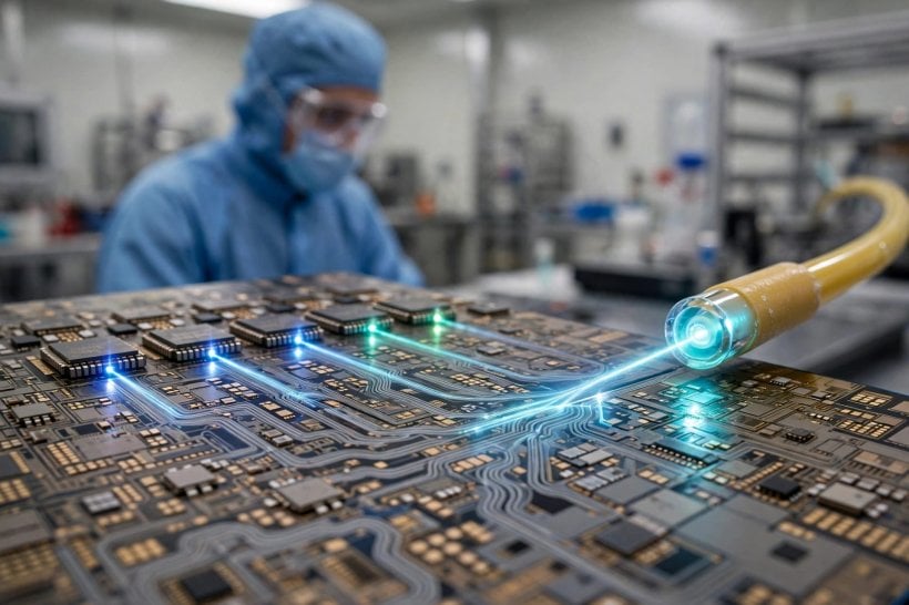
Photon Bridge’s Laser Design, In Detail
Photon Bridge develops high-power, multi-wavelength laser-source technology for next-generation optical interconnects in AI data centres. Its platform is designed to deliver high wavelength counts with up to 40 milliwatts of optical power per wavelength per fibre, while allowing production across multiple indium phosphide (InP) foundries.
Rather than generating the required optical power from a small number of increasingly powerful lasers, the company combines and multiplexes light from multiple lower-power semiconductor lasers. Lower power densities make individual lasers less sensitive to manufacturing defects, which improves production yield and lets the architecture scale more efficiently as volumes increase, according to the company.
That yield-first design is the heart of the pitch. Today’s high-power laser supply chain was largely built for telecom and subsea networks, where volumes are far lower. Photon Bridge argues that AI will transform the laser from a specialist photonics component into something that has to be manufactured at semiconductor scale, and that its architecture was designed from the beginning for those volumes.
Why Lasers Are Becoming An AI Bottleneck
As AI clusters expand from thousands to hundreds of thousands of processors, moving data between those chips is becoming a fundamental constraint on performance. Optical connections can move enormous amounts of data faster and more efficiently than conventional electrical interconnects, and they are consequently moving progressively closer to the processors themselves.
That shift is accelerating with co-packaged optics, which integrates optical connectivity directly alongside the chips that move data through AI systems. Omdia forecasts that more than 20 million data-centre AI accelerators will ship annually by 2028, and each generation of systems — from NVIDIA’s containerised DSX POD Vera Rubin factories to Google Cloud’s Vera Rubin A5X instances — packs more accelerators into tighter, faster fabrics. The more accelerators ship, the more laser sources the industry needs to light the links between them.
“Every new wave of compute creates new bottlenecks further down the supply chain, and lasers are the next one,” said Ion Hauer, Investment Partner at APEX Ventures. “Photon Bridge is addressing this with a technology that combines deep photonics expertise with a credible path towards manufacturing at very large scale.”
What Photon Bridge Plans To Do With The Money
Chief executive Paul Marchal, who joined when Photon IP rebranded as Photon Bridge in September 2025, framed the raise around scale. “We are moving towards enormous systems in which hundreds of thousands of processors have to operate together, and moving data between them is becoming one of the defining constraints on performance,” Marchal said. “The industry will soon need millions of these laser sources every year. Instead of making individual lasers increasingly powerful and difficult to manufacture, we move that scaling challenge into the architecture.”
Cesare Maifredi, Partner at 360 Capital, made the same point from the investor side: “Once you start talking about millions of units a year, manufacturing yield becomes fundamental. Photon Bridge has designed its architecture from the beginning around the volumes this market is going to require.”
The timetable is long by software standards. First samples are due in 2027, with volume manufacturing preparations following in 2028 — a schedule that reflects how qualification works in photonics, where a laser source must prove itself inside customer systems long before it ships in quantity, in the same broader build-out as the expanded Cosmos tooling NVIDIA announced for physical AI.
Why It Matters
Photon Bridge matters because the AI boom’s constraints keep moving down the stack. First it was accelerators, then memory and packaging substrates, then power and deployment time. Interconnect is the next constraint in line, and lasers sit at the start of the optical chain: without millions of reliable, manufacturable laser sources, co-packaged optics cannot scale, and clusters stall at the speed of their slowest links. A €10 million round will not solve that alone, but it puts a European specialist — founded in 2020 by Rui Santos and Xaveer Leijtens in the Eindhoven photonics ecosystem — into the race to supply the component the whole industry is about to need in semiconductor volumes.
Background
Photon Bridge was founded in 2020 in Eindhoven, the Netherlands’ photonics hub, by Rui Santos and Xaveer Leijtens to rethink how high-performance photonic systems are built at scale. It raised a €4.75 million seed round led by Innovation Industries in January 2025, rebranded from Photon IP to Photon Bridge that September and appointed Paul Marchal as chief executive. The new €10 million round brings in the Amadeus APEX Technology Fund and 360 Capital as co-leads alongside its existing Dutch backers.
Source: EU-Startups, Tech.eu




0 Comments